Component Foundations 5: Transistors
Learning goals
- I can name the base, collector, and emitter of a bipolar junction transistor.
- I can distinguish NPN and PNP symbols and roles.
- I can explain how a small input can control a larger load current.
- I can verify a real pinout instead of guessing from package shape.
What is a transistor?
A transistor is a semiconductor device used for switching or amplification. The bipolar junction transistors in the XL741 kit have three terminals:
- base (B): control terminal;
- collector (C): part of the controlled-current path;
- emitter (E): the other end of that path.
An NPN and PNP transistor operate with opposite polarities and current directions. They are not interchangeable.
A first switching circuit
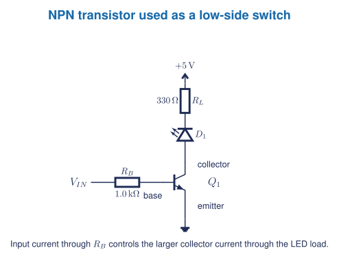
For a beginner switching model:
- off: base drive is absent, so collector current is approximately zero;
- on: sufficient base drive allows load current, subject to the load, source, transistor ratings, and saturation voltage.
This model is useful but incomplete. Transistor gain varies, and a switch design must provide adequate drive without exceeding base, collector, voltage, power, or temperature limits.
Package shape is not a pinout
Two transistors in similar packages may arrange base, collector, and emitter differently. Verify the exact manufacturer datasheet and the board marking. Installing a transistor backwards is a common kit fault.
The XL741 v2.0 uses thirteen 2N3904 NPN transistors and seven 2N3906 PNP transistors. The quantity itself is a useful lesson: an op-amp symbol can represent a system built from many individual devices.
Five-question starter
- Name the three BJT terminals and state the role of each.
- Explain why NPN and PNP transistors are not interchangeable.
- Trace the load-current path in Figure 1 when Q1 is on.
- Explain why both \(R_B\) and the LED load resistor are required.
- A transistor matches the package drawing but the circuit fails. Write a diagnostic sequence that checks part number, pinout, orientation, supply polarity, base drive, and current limiting without immediately replacing the part.
Jupyter and lab pathway
Start with an ideal two-state model in Jupyter or a circuit simulator. Sweep the input condition and predict load current from the source, LED model, and load resistor. Clearly label this as a model: it does not prove the selected transistor has adequate drive, safe power dissipation, or the expected pinout.
Physical testing uses a protected low-voltage supply and current limiting. The XL741 build comes later, after students can identify diode and transistor orientation and inspect solder joints.
Textbook support: Grob transistor and switching chapters, used with the matching Problems and Experiments Manual sections. [1, Chs. 28-30] Open Circuits provides classroom visual context for semiconductor construction. [2]